Voltage Controlled Quantum Phase
In graphene, a sheet of carbon atoms arranged in a honeycomb structure, charge carriers behave as massless Dirac fermions and possess exotic electronic properties. Especially, exceptionally high mobility (~105 cm2V-1s-1) and long coherence length (~1 μm) make it very attractive alternative channel material for future metal-oxide-semiconductor field effect transistors (MOSFETs).
Lack of a band gap in graphene is one of the biggest challenges for achieving high ON/OFF current ratios in graphene field effect transistors (FETs). The most obvious way to circumvent this problem is to open a band gap, e.g., by using chemical doping, creating nanoribbons, or by applying a vertical electric field in bilayer graphene. However, it is difficult to create a sufficiently large band gap without degrading the electronic properties of graphene. Another way is to utilize the unique properties of graphene in alternative FET architectures.
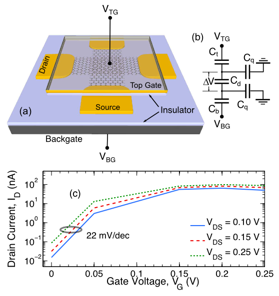
Quantum Phase Field Effect Transistor (QPhaseFET): (a) schematic diagram (b) capacitance model for electrostatics (c) transfer characteristics.
Currently, my research is primarily focused on design, simulation and modeling the quantum transport in novel bilayer Graphene based electronic devices that utilize the exotic properties of graphene. More specifically, we unveil a current switching mechanism in graphene crossbars in which the current can be modulated by several orders of magnitude. This switching mechanism is based on voltage control of the relative phases of the electronic wave functions of two crossed graphene nanoribbons.
We have demonstrated proof-of-principle calculations for a novel transistor consisting of crossed graphene nanorbbons. It exploits the voltage controlled quantum phase modulation, and does not require a bandgap or modulation of a potential barrier. Numerical simulations, based on the DFT and NEGF, show that the QPhaseFET operates with a steep inverse subthreshold slope (22 mV/dec) and high on/off current ratio (104). Since the QPhaseFET does not rely on the voltage modulation of a potential barrier, it is not limited by the fundamental inverse subthreshold slope of 60 mV/dec of the conventional MOSFETs. It operates below 250 mV at room temperature giving a significant reduction in switching energy. The active region of the QPhaseFET can be scaled down to 1.8nm × 1.8nm. This length scale is well below any horizontal scale envisioned in the International Technology Roadmap for Semiconductors (ITRS).